In this section, we look at the use of simple registers to control the flow of data in a computer system. One can, in fact, divide a computer CPU into two sections: the dataflow section, consisting of registers, busses and arithmetic/logic components, and the control section, containing steering logic, counters for state sequencing, etc. The control section is sometimes called the "glue" logic, as it connects to all the control points (CLEARs, LOADs, etc) of all the registers, octopus-like.
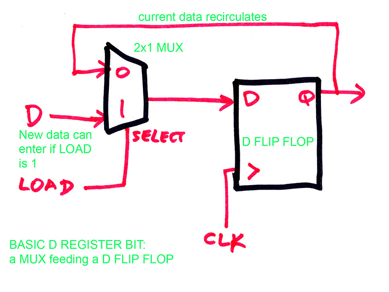
Just to review, the basic register bit is shown below:
The clock runs continuously. If LOAD is 0, the flip flops just keeps re-storing its old data and so doesn't change. If LOAD is 1, then new data will be stored. This diagram is a one-bit slice of a data register. The number of bits in the register is called the width of the register. This is commonly 8, 16, 32, or 64 bits. The registers and other arithmetic logic such as adders are interconnected with parallel busses. In parallel data transfer, the bits all run along similar wires simultaneously, and are stored in the register at the end of the bus at the same time.
(Q)This is really answered on a previous page. Why do we need this rather complex register bit design? Why can't we simply use a latch, saving about 70% of the transistors, and store the data by pulsing the ENABLE on the latch with the LOAD pulse? [As noted previously, this CAN be done, but....]
The diagram below shows the basic register dataflow connection:
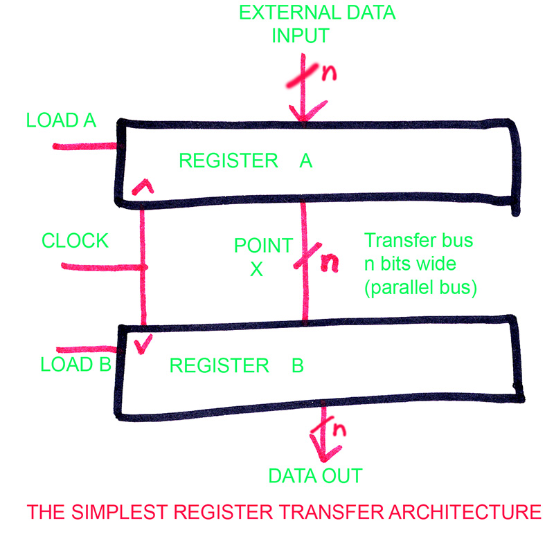
Here, data will be loaded from the external data input bus into register A if LOAD A is high when the clock edge arrives. Each register, and their busses, are n bits wide. In the x86 (IA32), for instance, the registers are 32 bits wide, so n is 32 in that case. The 32 bit register consists of the D register itself (see previous diagram) copied 32 times. Data moves in parallel-all 32 bits are transferred together, one into each register bit.
If LOAD B is high when the clock edge arrives, whatever is at POINT X will be transferred into register B. Normally, when the data is loaded into a register, it is visible at the output pins of the register after a short propagation delay through the latches in the register's flip flops. [It is possible to create "tri-state" registers in which an additional "tri-state buffer" is added to the output pins. This tri-state buffer is like a switch or CMOS transmission gate. This is used to allow multiple registers to be connected to the same output bus without electrical contention and without the need for multiplexers to select the desired register for connection to the bus]
If LOAD A and LOAD B are both 1 when the clock edge arrives, external data goes into register A and the previous data in register A (visible at POINT X) will be loaded into register B. This situation is referred to as a pipeline.
It seems rather useless to merely store the data and move it in this fashion, and this is generally true. Normally, at POINT X there is some sort of combinational logic, such as an adder or ALU, or some other logic.
The ACCUMULATOR topology is shown below:
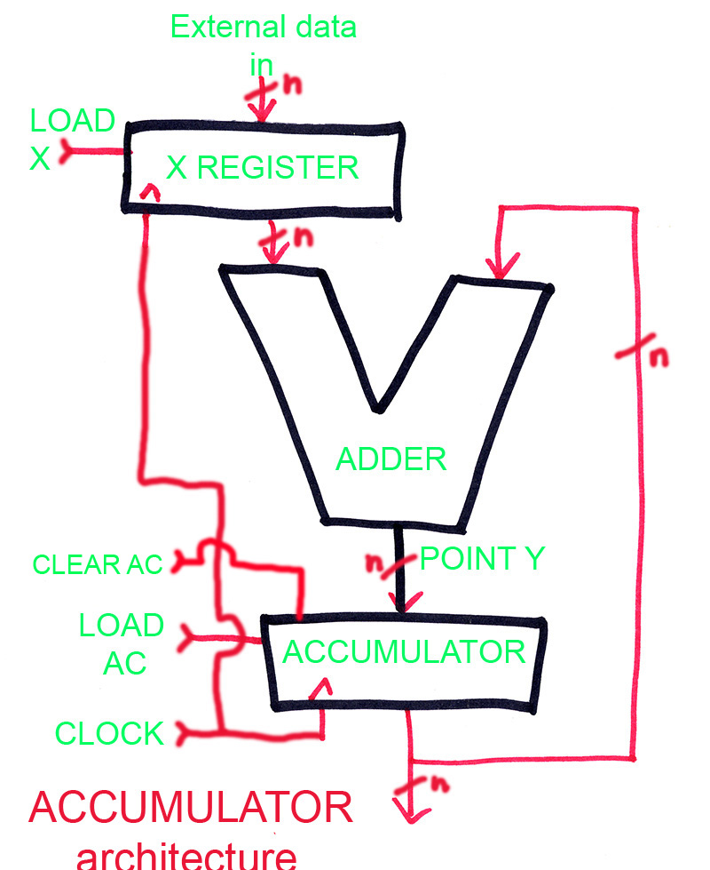
Here, new data can be brought in through the X register and added in to the accumulator. This sort of thing is the basis of many simple CPU architectures. We can think of data flowing through the architecture, controlled by the LOAD signals. I will repeat again that there is nothing critical about the timing of the LOAD signals except that they must be in the desired condition at the clock edge, and just before that (setup time) and just after (hold time) to avoid incorrect operation and possible (although unlikely) metastability.
So, when new data is loaded into the X register, it propagates into the adder, where all electrical hell breaks loose as the current value of the accumulator register is added to this new data, carries are propagated, etc. Finally, everything settles down electrically, there is a stable sum sitting at POINT Y. [The adder is guaranteed to settle after some finite time since it contains no feedback or loop paths internally.] This sum of course doesn't get into the accumulator register, as that register is not transparent, being made of edge triggered flip flops. If LOAD AC is active when the next clock edge arrives, then the sum will be stored in the accumulator. Immediately, all hell breaks loose again, as the new output value feeds back into the adder. Also, we will likely be bringing new data in too at this time.
(Q)What sequence of events is needed to use the accumulator topology to add two numbers?
In order to understand the data flow, we need to say more about timing diagrams. Below, we see the conventions I will use in this section:
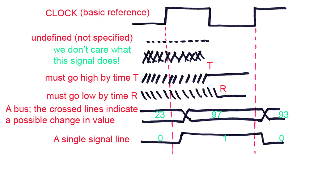
So, let's look at a timing diagram for the process described above.

The algorithm for tracing the operation of any synchronous circuit is to determine the inputs to all flip flops (registers) when the rising edge of the clock arrives. Those values on the D inputs of the actual flip flops will be transferred into the flip flops at that time (actually just after the rising edges, owing to propagation delays).
So, we are assuming that at the start of the time being analyzed by this diagram, we have a value of 10 in the ACCUM register, with 27 sitting at EXT INPUT, where it is loaded into X REG by rising edge 0. We are now in STATE 1, which runs from just after the edge that ended state 0, to just after the rising edge labelled 1. During state 1, sufficient time must be allowed for all flip flop inputs to become stable, so as to satisfy the set up time requirement. We see that the 10 from ACCUM and the 27 from X REG have flowed into the adder, resulting in a cascade of electrical disturbance indicated by the crosshatch at POINT Y. Fortunately, we don't care about this, so long as it clears up (i.e. the carries all settle within the adder) before the set up time for the clock at 1. We see that the value 37 settles well before the dotted red line ending state 1, so the 37 is loaded into the ACCUM.
Meanwhile, the same clock edge transfers 35 from the external input into X REG, where it flows into the other port of the adder. Once again, all hell breaks loose as the adder output settles, and the sum of 72 stabilizes, where it can be transferred into ACCUM at edge 2 of the clock.
I have shown all LOAD signals active for all clock edges. For a fully enabled pipeline, this is how it would work. Note the crosshatch on the LOAD signals. We don't care what garbage is on them so long as they are stable for the setup and hold times for the flip flop inputs.
Where do the LOAD signals come from? They are the outputs of the control section. What are the inputs for the control section? There are basically three groups: the outputs of a counter, the output of the instruction decoder, and any data-dependent feedback from the data section for data conditional operation, such as conditional JUMP instructions in the x86. All this is studied in detail in CPSC 401.
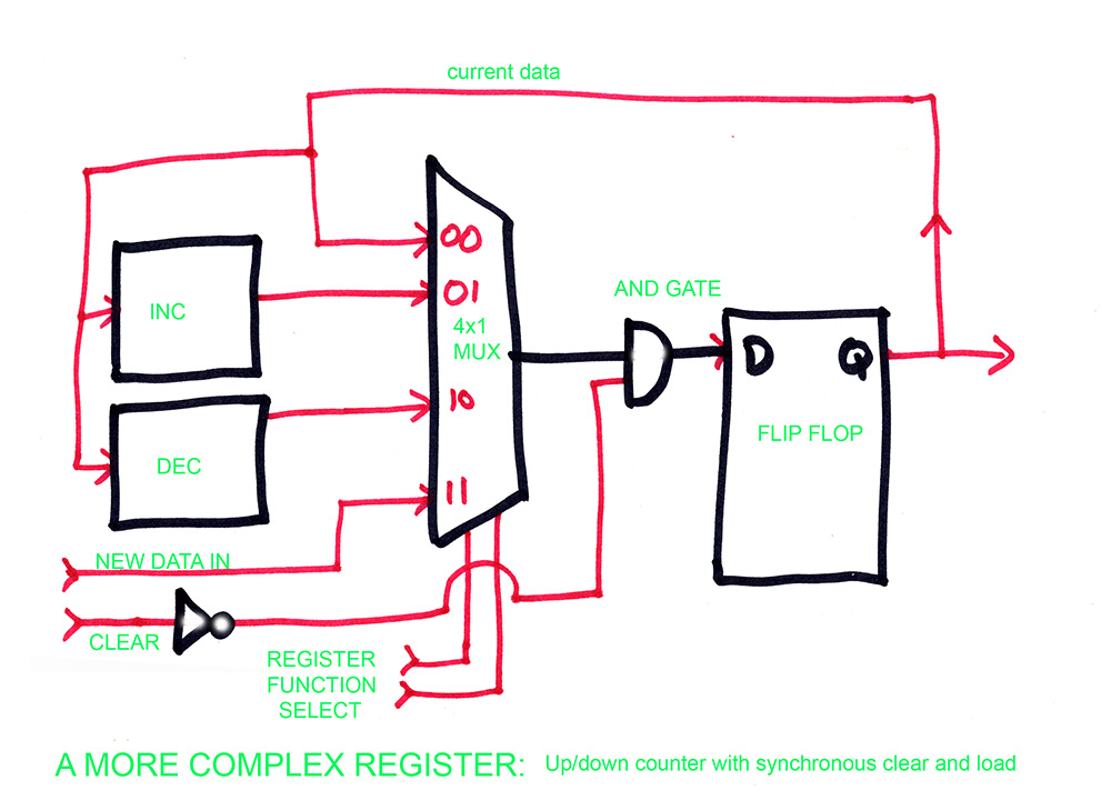
The diagram below shows another timing diagram, this time for the counter device shown earlier:
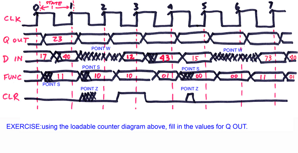
Remember the basic algorithm:look at the situation just before the clock edge; that situation will determine what will happen to the flip flops when the clock edge arrives.
(Q)The D input is shown as garbage at two points labelled POINT W. Why is this not a problem?
(Q)The function code inputs show crap (sometimes called "glitches") at POINT S. Why is this not a problem?
(Q)The CLR input shows glitching at POINT Z. Why is this not a problem?
(Q)Is the situation in State 3 ambiguous? Explain.
(Q)The Q OUT values are shown as being fully clean. Is this realistic?
(Q)The Q OUT values change after a noticeable delay after the rising edge of the clock. Many textbooks, misleadingly in my opinion, show this change right on the clock edge. Why is my representation more realistic?
(Q)Some registers allow for an asynchronous clear-the clear control input is directly connected into the flip flop itself to force a clear as soon as the clear input control signal is active, independent of the clock. In view of the timing diagram shown, why would this type of thing be a poor choice here?
(Q)Sketch a timing diagram for a 3 bit counter counting up from 000 for a full cycle. Show the clock and the Q OUT and Q'OUT signals. Use individial signal representation for the Q and Q' OUT, and also bus representation.
(Q)For the counter diagram shown above, show the timing of all the signals if we wish to initially load a value of 25 in the counter, increment it for 5 clock cycles, i.e. 25, 26, 27, 28, 29, 30, then clear the counter, and then decrement for 3 cycles. Assume it is an 8 bit counter.
This material is covered by MANO2 and MANO3 very differently to the treatment given on this page. Their material is in Chapter 7-8 of MANO2 and Chapter 8 of MANO3. The text by MANO: Computer Architecture (ISBN 0-13-175563-3) used in CPSC 401, Chapter 4, is useful here, and the earlier chapters of this book give a good quick review of the CPSC 321 material.