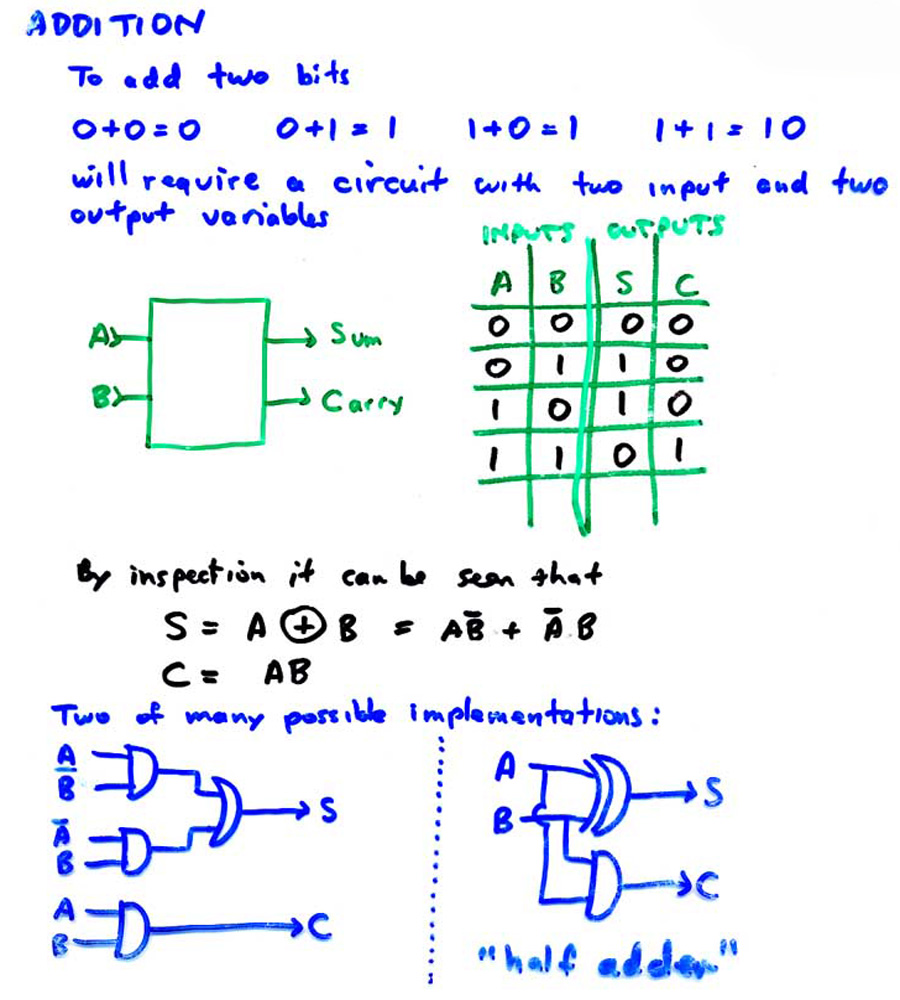
Now, we can see how the rather dry material on the previous page may be applied to create something that can do something useful for us. We start with the simplest case, adding two bits:
We see that we need a logic module with two inputs and two outputs, that is, two functions of two variables. These are shown at the bottom of the diagram above.
However, we need to add bigger numbers than 0 and 1. To do this, we add an additional input, a carry in, to make the 1 bit adder expandable to more bits.
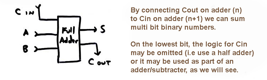
The implementation is shown on the next diagram:
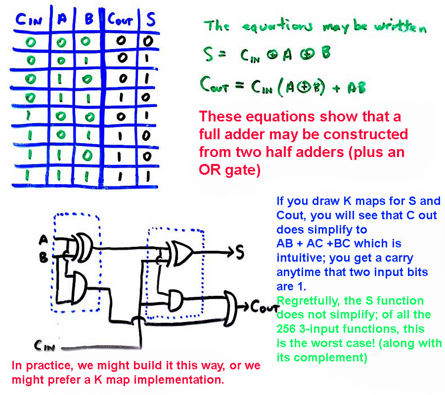
The relationship between XOR and arithmetic recurs in many contexts. If you draw the K maps, we see that
S = A'B'C + A'BC' + AB'C' + ABC
The K map looks like a checkerboard. No simplification is possible. The Cout function, however, does simplify.
(Q)Sketch the K maps for the full adder and show the simplifications.
(Q)Explain the design of the half adder and full adder. Why is the half adder insufficient?
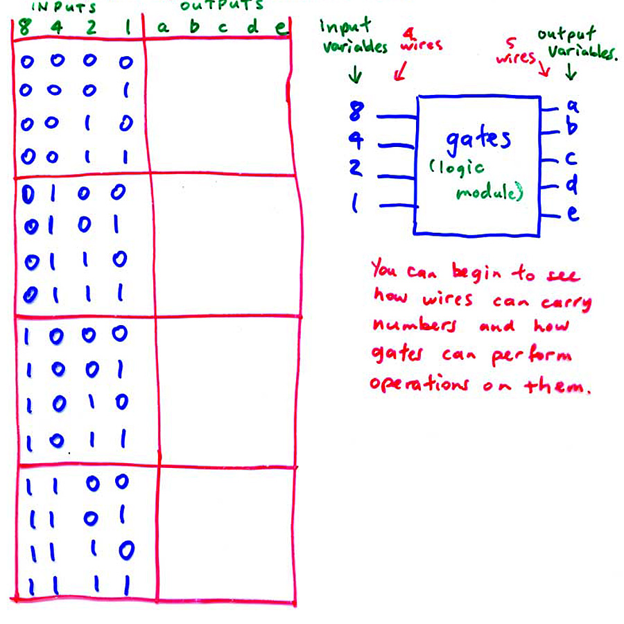
Could we just draw up a big truth table for a 16-bit adder, for example? It would require 33 input variables, if we allow a Cin to allow for expansion to 32 or more bits. There would be 17 functions needed; the 16 S bits and the Cout. The short answer is that it is totally impractical; firstly, to do the simplification, and secondly, to actually build it this way. I will discuss this more fully in lectures.
(Q)Discuss the issue of implementing a multi bit adder directly as a group of functions, rather than using the "daisy chain" algorithm to be discussed below.
The connection of a basic multi bit adder is shown below:
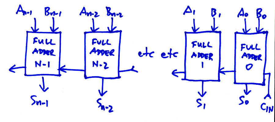
This topology is called the "ripple carry" adder. It is the slowest and cheapest adder. We can add one XOR gate per bit to this to make a 2's complement add/subtract unit, since A-B = A + B' + 1 using 2's complement representation. This economy explains the persistance of 2's complement arithmetic in binary computers.
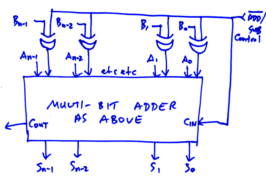
The control line ADD/SUB with the bar over the ADD indicates that the ADD is active low; that is, the unit adds if that line is 0, and subtracts otherwise. Note that 2's complement subtraction requires that we flip the bits on the minuend (the B in A-B) and add 1 to the final result. An XOR gate acts as a conditional bit flipper-sketch the truth table to see this-and the add 1 can be accomplished conditionally by simply connecting the control line to Cin. If the control line is 0 (add) the Cin has no effect on the result; if the control line is 1 (subtract) then the result is increased by 1.
We can begin to get a hint of computer design here. The ADD/SUB control line can be derived from bits in the instruction word of the system.
A tremendous amount of work has gone into optimizing real adders using the various different computer technologies over the decades. Gate level optimizations (such as in the Cout full adder function above) are possible. A major problem is in the carry propagation; if we are adding 11111111 + 00000001 the rightmost 1's propagate a carry to the next leftmost bit, which in turn propagates a carry up the chain, right up to the Cout of the 8 bit adder. This is rather slow; we could say that the carry delay is of order N where N is the adder size. This can be reduced to order logN by the use of a lookahead carry circuit, not discussed here. See the (321 pages if you are interested).
Further optimizations below the gate level are common; in CMOS, special function gates such as adders are common as "standard cells" for VLSI design. [Electromechanical relays allow all sorts of optimizations; multiple switches can be stacked onto one relay, as is visible in the photo above.]
(Q)Sketch a circuit for a 4-bit adder. Explain the modifications needed to make it a 4-bit add/subtract circuit.
(Q)Explain how an XOR gate can be a conditional bit flipper. Easiest way is to base your answer on the XOR truth table (F6 above).
(Q)Why have binary computers used the 2's complement method of representing integers?
(Q)Explain the problem of carry propagation delay. BONUS Sketch and explain the carry lookahead circuit.
MANO2: p116-123; p152-157
MANO3: p119-128
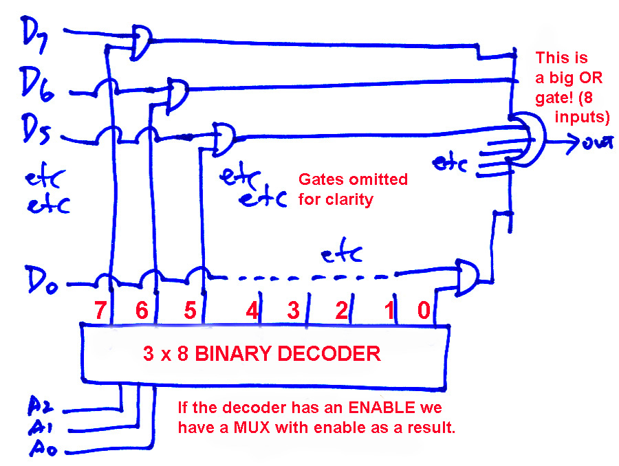
This is a very important logic module, being the basis of any system that must select data, e.g register selection logic, memories, etc. The basic module diagram is
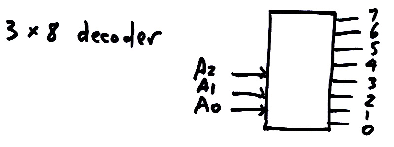
I have called the inputs A2, A1 and A0, corresponding to "address line" 2, 1, and 0. The address lines may be thought of as three-bit pointers to the active output. At any one time, only one output is active (i.e. 1) while the other seven outputs are 0 (inactive).
Internally, we have
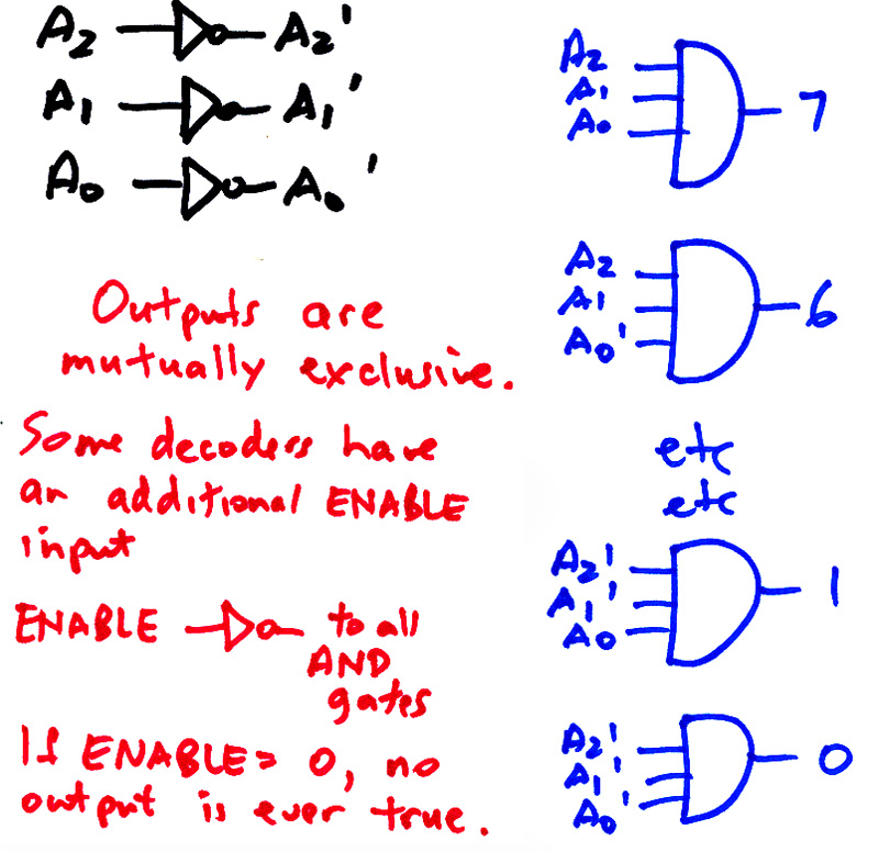
This diagram follows the usual convention for wiring ("schematic") diagrams, in that wires ("nets") with the same name are assumed to be connected.
As mentioned, the binary decoder has the property that the outputs are mutually exclusive. This is obviously important for data selection. However, it is certainly possible to design decoders with non MUTEX outputs! See the BCD to 7-segment decoder discussed below.
The multiplexer is the basic data selection device. Its module diagram is
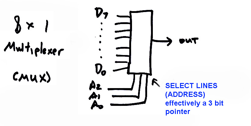
The internal diagram shows a 3x8 decoder enabling gates that allow external data (D7, D6 etc) to propagate to the output. The MUTEX property is guaranteed by the decoder.
[An interesting sidelight is that the MUX can be used to implement Boolean functions! If the inputs are hardwired to 0s and 1s and the function inputs are connected to the address lines, then we have a function generator. To implement F(x,y,z) = Sum (0,1,3,6,7) we would just connect address lines A2 A1 A0 to X Y Z respectively, and D7..D0 to 1 1 0 0 1 0 1 1. As it happens, this is rather wasteful. With the possible addition of an external inverter, it is possible to do this function using only a 4x1 MUX rather than an 8x1 MUX, for a saving in hardware of about 70%. The 321 pages give the algorithm for designing this way. Since this sort of thing is essentially obsolete for practical real-world hardware, I omit it from this course. (Some families of field programmable logic have used MUXes for the basic function generators. It seems a bit odd to think of making a 4 bit adder out of a few 8x1 and 4x1 MUXes, but it can easily be done.)]
(Q)Sketch circuits for the binary decoder and multiplexer. Explain their operation.
(Q)BONUS Sketch the implementation of the full adder functions using a pair of 4x1 MUXes, with additional inverters as needed. Method is given in the 321 pages and in MANO.
MANO2: p166-170; p173-175.
MANO3: p134-138; 141-144.
An example here is the BCD (binary coded decimal) to 7-segment decoder. Here is its basic module symbol:
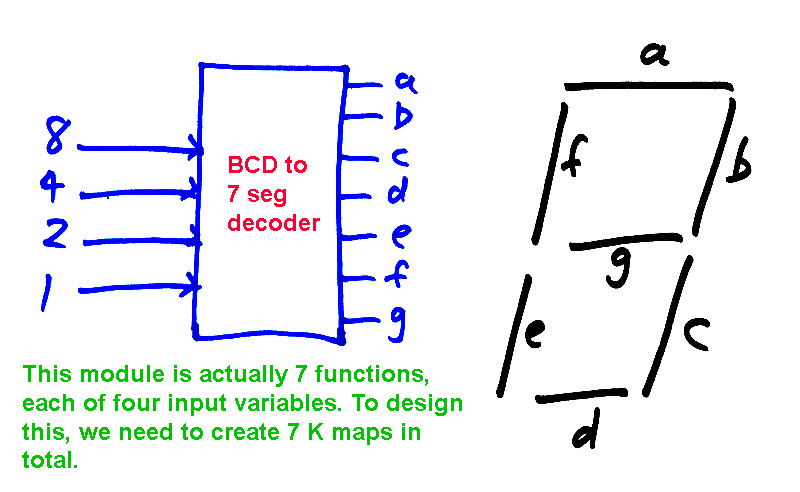
The diagram shows some of the design process.
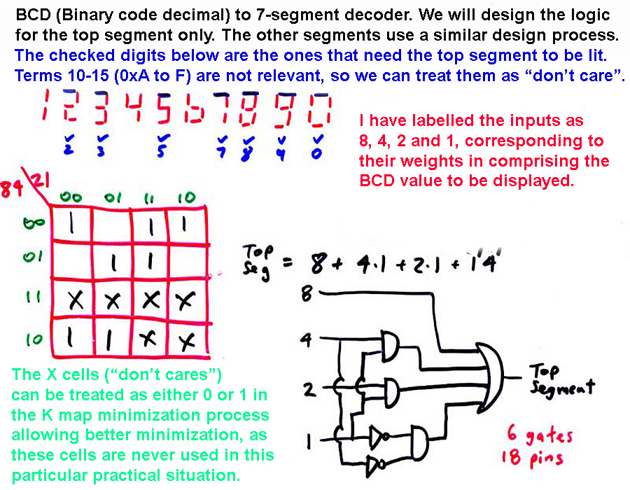
As you can see, we certainly DON'T have MUTEX here!
(Q)Design the other segment decode logic not implemented in the work shown here.
MANO2: p124-126;
MANO3: p116-118;
A decoder with ENABLE can be connected as a DEMULTIPLEXER, in which the ENABLE is the data input, the address lines work as usual, and the decoder outputs 7..0 are the data outputs D7..D0.
(Q)Explain the operation of the DEMUX.
We can also define an encoder, e.g. an 8x3 priority encoder. It takes 8 input lines, and returns the 3 bit binary number corresponding to the highest, or lowest, depending on the design, currently active input line.
Also, we can construct memories, which are basically decoders with storage cells associated (We look at these storage cells in the next page of these notes).
Another module is the comparator, which for example compares two 4-bit binary values and indicates >, < or =.
We will not look into these, for lack of time. As usual, information about them is in the 321 pages.
(Q)BONUS Sketch and explain ONE of: 8x3 encoder, 4 bit comparator, 8 bit equality-only comparator.
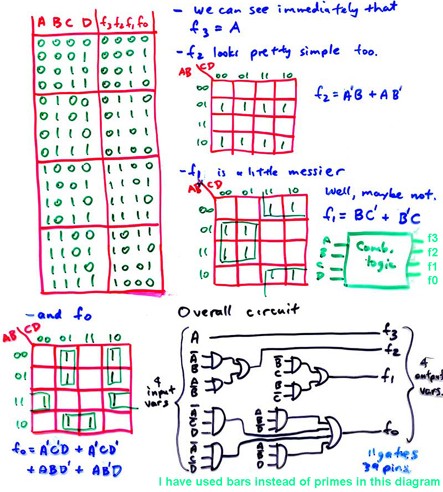
Example 1. Design a 4 bit circuit to map a 4 bit binary number (nibble) into a sort of reflected code sequence as tabulated in the truth table below:
(Q) Example 2. Design a minimized combinational circuit that will add 9 to a 4-bit number. We could use a "MSI" (medium-scale integration) approach here, in which we take a 4 bit adder, tie one input to 1001 (i.e. 9) and connect the 4 bit number to the other input. However, this question asks for a minimized solution, so we will create a truth table and use K maps to find the functions. The basic setup is shown; the actual implementation is left as an exercise.
To design arbitrary combinational logic, we need to obtain the truth table, then implement the logic using K maps, etc. Logic with too many inputs for truth table methods, such as a 4 bit adder or a 4-bit comparator, requires an algorithmic approach. You are responsible for the examples in these notes, plus any additional ones discussed in lectures.
Many examples are given at the ends of Chapters 3 and 4 of the MANO texts; a number of these have solutions at the back of the books.